Compound semiconductor material products are at the core of advances in technology, impacting our daily lives. These products offer great benefits, but the manufacturing process still remains environmentally, sustainably and financially undesirable.

It is impossible to modify the compound semiconductor manufacturing process. However, reducing total production costs and enhancing yield through improvement to ancillary support maintenance processes is possible.

A Green Technology?

The epitaxial process used for creating the semiconductor material, the first stage of LED manufacture, is the most expensive because it is a very complex process in its own right. The specialist manufacturing techniques used (such as CVD) are intensive, requiring a high level of skill and control. Furthermore, beyond requiring specialist equipment, the process has high power use, requires expensive specialist chemicals, and is a very intensive process.

In particular, the chemical reagents required are not only expensive in their own right, but highly toxic and have a significantly intensive production process of their own, including their own manufacturing impact on the environment. This is not to mention the toxic waste produced by compound semiconductor manufacturing processes that has to be carefully processed, again chemically, and disposed of.

So, although compound semiconductor products may be leading greener, more sustainable applications at point of use they have significant environmental impact footprint at point of manufacture. This is the source of the semiconductor paradox.
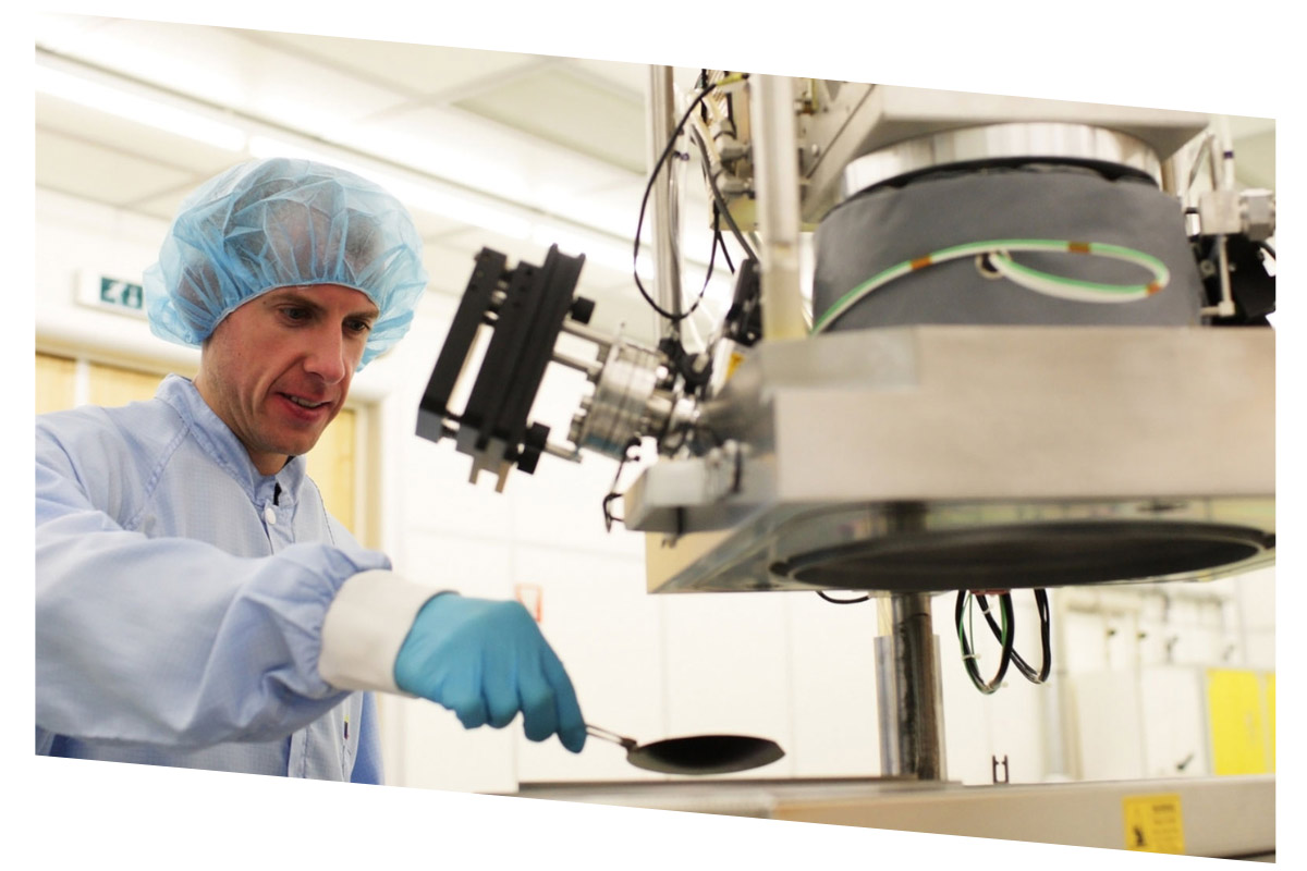
Aesin Ltd. has developed a process tool intended to clean susceptors, satellites, etc. from MOCVD systems used for the deposition of AlN, GaN, InN, etc. to manufacture LED’s or other devices.

Aesin Ltd. has developed a process tool intended to clean susceptors, satellites, etc. from MOCVD systems used for the deposition of AlN, GaN, InN, etc. to manufacture LED’s or other devices.

The Compound Semiconductor Constraints

Semiconductor epitaxy is a complicated engineering feat, requiring specialist knowledge and specialised equipment. In order to repeatedly produce material of high quality the process is required to be absolutely stable and reproducible. A single lost material production run can result in $100k’s of loss. To mitigate this, a locked down process, often called copy exact, is used by producers to achieve cost effectiveness in this expensive process.

In this approach it is paramount that all process parameters must be same, all chemical inputs to the process identical and most importantly that the condition of the reaction chamber at the start of each process is identical from process to process. This means that all components inside the chamber need to be maintained to an absolute cleanliness standard ensuring material production is not affected by their condition.

Sub-standard maintenance or degradation of the chamber components over time have a major impact on yield (the amount of high-quality material produced by the system in a single process) and hence, significantly reduce profit. A poorly maintained reactor or degrading components is a very costly situation in compound semiconductor material production.

The Maintenance Process

It is therefore extremely important that the reactor components, or ancillary parts are maintained to a very high standard, so as not to adversely affect the material production process. However, this can be a challenging prospect given that the components get very dirty, becoming heavily coated with process by-product.

In most situations, so as not to disturb the condition of the production reactor and potentially impact the production process, component cleaning happens externally to the material production system. Ancillaries are removed and transferred to another system to ensure no contamination of the production chamber can occur.

The process for maintaining the ancillaries is an aggressive one. The need to remove compound semiconductor waste material from a component is naturally more intensive than the process required to create it. To achieve complete component cleaning this routinely requires a very high temperature (way in excess of the material production temperature) chemically assisted, using aggressive etchants, with long processing times (several times longer than the material production time). The procedure requires expensive specialist equipment, which itself is costly to maintain, as it operates at extremes of temperature and frequently pressure.

The consequence of such rigorous maintenance procedures is the over-stressing of the system components, resulting in significantly shortened lifetime.

Due to the intensive nature of the cleaning process for the manufacture of some compound semiconductor material the ancillary cleaning process can account for up to 40% of the epitaxy cost. Even more when the shortened lifetime of the components and the maintenance of the cleaning equipment itself, is taken into account.

Furthermore, the demands of the process require very high power over long periods of time (> 10 hours), with undesirable chemicals producing significant amounts of toxic waste and CO2 emissions. Additionally, the process shortens the lifetime of components which cannot be recycled resulting in increased waste of expensive component materials, making this part of compound semiconductor production extremely detrimental to the environment.

Improving the Compound Semiconductor Manufacturing Process

So, the current process used to maintain components is very much a sledgehammer approach, but it works and is a trusted procedure that leads to repeatable, reproducible material production. However, its less than desirable high cost and significant environmental impact offer the opportunity to both significantly decrease the overall cost of manufacture and reduce environmental impact of compound semiconductor materials production, with the correct engineering solution.

As highlighted the three main issues of the current standard process are:

  • Very high temperature
  • Long process time
  • Harsh system ambient

A reduction in any of these factors would reduce energy consumption, reduce inventory requirement, with all the positive benefits this has up the value chain, reduce material waste, increase component lifetime and most importantly increase compound semiconductor material yield.

A solution to all three of these issues is now possible in a single system, in the form of the Aesin ReClean.

This new approach to compound semiconductor production system component maintenance employs a low temperature, chemically assisted, cleaning process that reduces cleaning time down to < 3 hours. The significantly less aggressive nature of the ReClean, and the reduced processing, or part exposure, time means it is less harsh on components and turnaround is massively reduced. Furthermore, spare part inventory can be reduced.

The process returns components to near new condition and the uniform nature of the procedure means that ultimate yield can be achieved in the following production process.

The system itself requires very little maintenance again due to its less aggressive process.