
Founded by CTO, Andrew Humphris, Infinitesima is an Oxfordshire based supplier of in-line and lab based probe metrology tools for advanced semiconductor manufacturing.
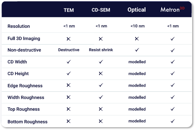
Metrology is essential to maximise the yield, and hence cost efficiency of Semiconductor fabrication. Technology inflections towards High NA EUV, hybrid wafer bonding, and complex 3D device structures are now moving beyond the capability of existing e-beam and optical techniques and are a limiting factor for further progress.


Our key product, the Metron3D system is a fully automated, sub-nanometer, high-speed 3D imaging system, operating at production throughputs of up to 170 wafers per hour.
- Throughput and imaging speeds up to 100x faster than conventional atomic force microscopy Patented photo-thermal actuation of the probe tip
- Fully automated for high throughput in-line operation
- Wide field of view optical global align system
- High-speed 600 mm/s wafer stage
- Probe library with fully automated probe exchange and 25 probe capacity
With imaging time measured in seconds rather than minutes, the system is installed in leading IC manufacturers to address metrology challenges for manufacturing next generation logic, DRAM and 3D NAND devices.
Application Highlight – Wafer Bonding
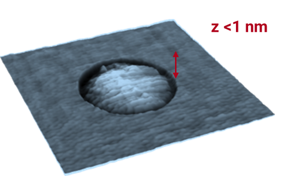
Wafer bonding of high-density contacts for next-gen devices requires precise sub-nanometre control of contact pad height to ensure all contacts are mated
Challenge
1. E-beam metrology does not deliver z-height information
2. Optical systems have limited lateral resolution
3. AFM is too slow
Solution: Infinitesima Metron3D
Precision sub-nanometer imaging of contact pads


The Future
Further developments are underway and we are excited to be looking to the next innovations on the roadmap as we work towards a further order of magnitude improvement in imaging speed.
Multiplexed optics and parallel scanning probes provide a scaling roadmap towards a further order of magnitude increase in imaging speed, enabling large area metrology and inspection applications.
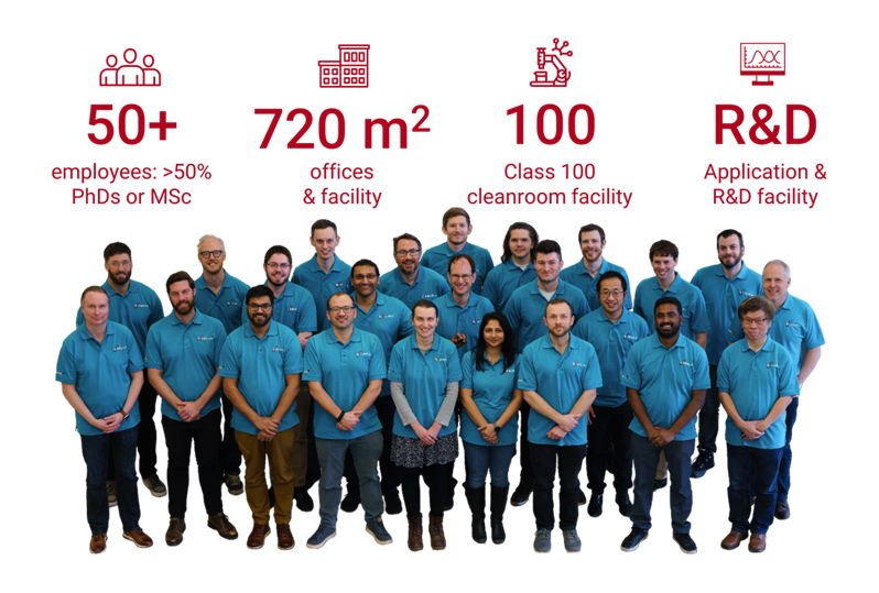
Industry Experts and Technical Leaders

